
Silicon chip
Updated: 10/17/2017 by Computer Hope
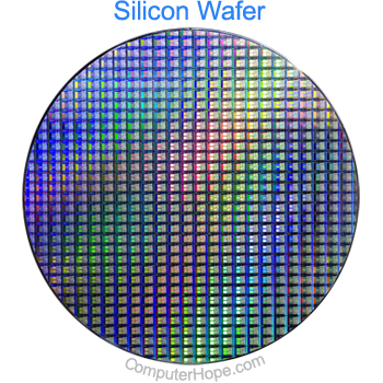
A silicon chip is an integrated circuit made primarily of silicon. Silicon is one of the most common substances used to develop computer chips. The picture shows an example of a silicon wafer with several individual silicon chips.
Steps on how Silicon is formed into chips
- Silicon is formed into pure silicon crystals using the Czochralski method, which uses electric arc furnaces to transform raw materials (mostly quartz rock) into metallurgical grade silicon.
- To help reduce any impurities the silicon is converted into a liquid, distilled, and then formed back into rods.
- The rods or poly silicon is then broken up into chunks and placed into a special oven that is purged with Argon gas to eliminate any air. The oven melts the chunks when heated to over 2,500° Fahrenheit.
- After the chunks melt, the molten silicon is spun in a crucible while a small seed crystal is inserted into the molten silicon.
- While continuing to spin and cool the seed is slowly pulled out of the molten silicon resulting in one large crystal. Often weighing more than several hundred pounds.
- The large silicon crystal is then tested and X-rayed to make sure it is pure.
- If the crystal is pure it is cut into thin slices called wafers, like the one shown on this page.
- After being cut, each wafer is buffered to remove any impurities that may have been caused when it was sliced.
- Once all buffering is completed, the wafer is inserted into a machine that etches the silicon with the circuit design. These designs are etched using a process called photolithography.
- Photolithography works by first coating the wafer using a photo sensitive chemicals that harden when exposed to UV (ultraviolet) light and then exposing the wafer to the chip design layer using a UV light.
- After being exposed, the remaining photo sensitive chemicals are washed away leaving only the chip design. After the chemicals are washed away, the layer may be cooked, blasted with ionized plasma, or bathed in metals. Each chip design has multiple layers, so the photolithography steps are repeated several times for each layer until complete.
- Finally, each silicon chip is sliced from the wafer.